

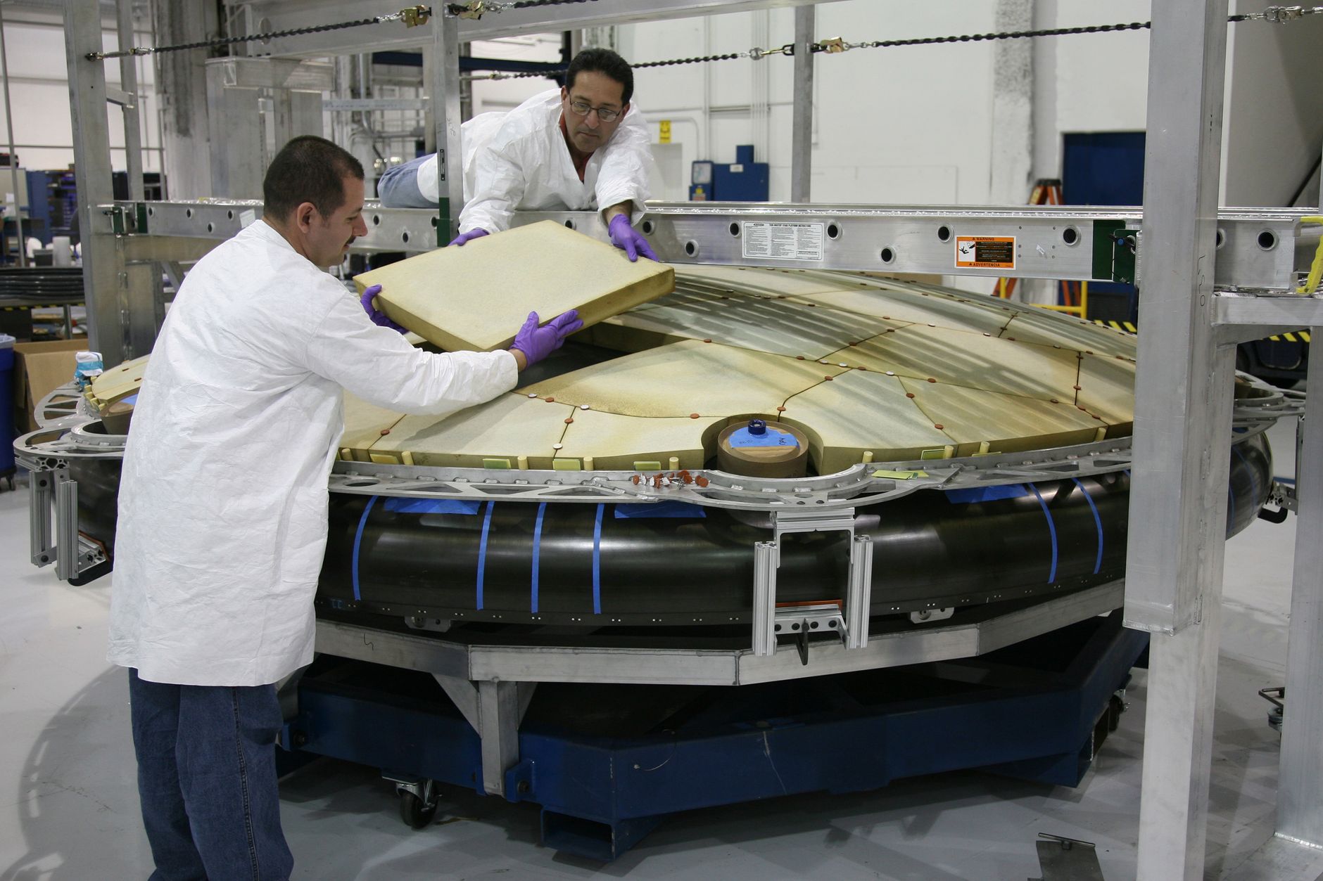
Space vacuum manufacturing is a groundbreaking approach being tested by Besxar for GaN wafer production. This innovative technology could revolutionize how materials are processed in space environments.
What is Space Vacuum Manufacturing?
Space vacuum manufacturing is an innovative technique that leverages the unique conditions of outer space to produce materials with enhanced properties. By utilizing the vacuum of space, manufacturers aim to minimize contamination and defects that typically occur during the production process on Earth.
This method is particularly promising for the production of Gallium Nitride (GaN) wafers, which are essential components in various electronic devices, including high-frequency and high-power applications. The vacuum environment allows for a more controlled manufacturing process, which can lead to higher quality wafers with improved performance characteristics.
In space, the absence of atmosphere reduces the likelihood of impurities and allows for more precise control over the manufacturing conditions. This can result in:
- Reduced Defects: The vacuum environment minimizes the introduction of contaminants.
- Enhanced Material Properties: Wafers produced in space may exhibit superior electronic properties, making them ideal for advanced applications.
- Cost Efficiency: Although initial setup costs can be high, the long-term benefits may outweigh these investments.
As companies like Besxar test the feasibility of space vacuum manufacturing for GaN wafers, the potential for revolutionizing electronics manufacturing in space continues to grow, promising advancements that could significantly impact the industry.
Benefits of GaN Wafers in Space
Gallium Nitride (GaN) wafers are increasingly recognized for their pivotal role in advancing space technology, particularly in the realm of electronics and power devices. The unique properties of GaN make it a superior choice for high-performance applications, especially in the harsh environment of space.
- High Efficiency: GaN wafers offer significantly higher efficiency compared to traditional silicon wafers. This efficiency translates into less energy loss, making them ideal for power amplifiers and converters used in satellites and spacecraft.
- Thermal Stability: The ability of GaN to withstand higher temperatures without degrading performance makes it suitable for environments where thermal management is critical, such as in space missions.
- Compact Design: Devices manufactured from GaN wafers can be smaller and lighter, which is essential for reducing the overall weight of space equipment.
- Radiation Resistance: GaN materials exhibit greater resistance to radiation, a crucial factor when considering long-duration space missions that expose components to cosmic rays and other forms of radiation.
Utilizing space vacuum manufacturing for GaN wafers could enhance these benefits further, ensuring that the production process maintains the integrity and quality necessary for such demanding applications. As research continues, the potential for GaN technology in space operations appears increasingly promising.
How Does Besxar Test This Technology?
Besxar employs a multi-faceted approach to test the effectiveness of space vacuum manufacturing in the production of GaN wafers. This process begins with the careful selection of materials that can withstand the unique conditions of space, ensuring that the wafers retain their integrity during manufacturing.
To evaluate the technology, Besxar conducts a series of experiments that simulate the vacuum of space. These tests assess the behavior of GaN materials under various temperature and pressure conditions. By utilizing advanced sensors and monitoring equipment, the team collects data on how these materials react to the space environment throughout the manufacturing process.
Key components of Besxar’s testing protocol include:
- Vacuum Chambers: Specialized chambers replicate the low-pressure conditions found in space, allowing for precise experimentation.
- Thermal Control Systems: These systems manage temperature fluctuations, simulating the extreme thermal environment encountered in space.
- Real-Time Monitoring: Continuous data collection ensures that any anomalies can be quickly addressed and analyzed.
Through these rigorous tests, Besxar aims to establish a reliable methodology for space vacuum manufacturing, paving the way for higher quality GaN wafers that could enhance performance in space applications. The results of these tests will be crucial in determining the feasibility of utilizing this innovative manufacturing method in future space missions.
Future of Space Manufacturing Techniques
The future of space manufacturing techniques holds significant promise, particularly with the advancement of space vacuum manufacturing. As research continues, it is becoming clear that this method may transform the production of materials, especially in the context of gallium nitride (GaN) wafers.
One of the key advantages of using space vacuum manufacturing is the ability to create materials in a low-gravity environment, which can lead to enhanced material properties. This unique setting allows for:
- Improved purity: The lack of atmospheric interference reduces contamination, resulting in higher-quality wafers.
- Better crystallization: The microgravity environment can facilitate more uniform crystal structures, crucial for electronic applications.
- Energy efficiency: Manufacturing in space can potentially reduce the energy required for certain processes, as the vacuum environment reduces thermal losses.
Moreover, as companies like Besxar continue to test and refine this technology, the potential applications for GaN wafers in both terrestrial and extraterrestrial environments expand. As the aerospace industry pushes for more efficient and advanced materials, the integration of space vacuum manufacturing techniques will likely play a pivotal role.
In conclusion, the evolution of space manufacturing techniques, particularly through the lens of space vacuum manufacturing, is set to revolutionize how materials like GaN wafers are produced and utilized in the future.
Photo by SpaceX on Pexels
Read the original
You might also like
- Vivo X500 Launch: The Best Smartphone with Zeiss Cameras
- Googlebook laptops: Best features and price details
- Affordable 5G Smartphone: Best Real Value with Lava’s Virat Curve